


Growing demands on high-speed data communication, unmanned aerial vehicles and portable medical devices are attracting industries to new manufacturing methods like, for example, Nanoscribe’s direct laser writing technology. Currently, the production of photonic circuits and microelectromechanical systems (MEMS) needed for these applications requires different manufacturing methods and multiple process steps for bringing together various components on one microchip.
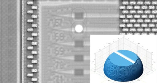
Snapshot of the 3D printing process of a hemispherical lens on a chip. Inset: Print simulation of the 3D component. Image: Nanoscribe
Now, with Nanoscribe’s highest resolution 3D printers one can print and integrate microscopic components directly on integrated circuits such as micro-lenses onto photonic circuits and deformable structures on MEMS actuators. With this groundbreaking technique smallest objects with complex geometry and feature sizes from hundreds of nanometers up to several millimeters can be printed. They are produced in a single printing step and on a scale which was inaccessible to 3D printing before. This major update of on-chip printing brings new perspectives for producing nano- and microscale 3D components in situ, exactly where needed.
For this 3D printing process, Nanoscribe’s Photonic Professional GT system uses the method of two-photon polymerization. The precision optics and advanced software tools of this 3D printer allow to fabricate 3D polymer structures with submicron precision, making the strengths of additive manufacturing available to micro- and nanofabrication. These advantages are the full 3D design freedom and a simple workflow from CAD model to final part resulting in rapid design iteration cycles that save time and costs during product development.
Additionally, the wide choice of print surfaces now also includes pre-patterned chips making miniaturization of 3D functional parts into highly integrated circuits possible.
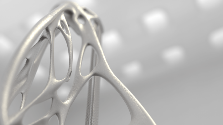
Nanoscribe_MEMS_BostonUniv The 3D printed micromechanical bowties are structures that stretch and deform in 3D due to their geometry. The scientists were able to deform the microstructure by applying a voltage to the MEMS actuator. Professor White states: “We show that coupling 3D microprinting with MEMS actuators is a powerful way to produce 3D micromechanical systems tailored to specific needs. Nanoscribe 3D printers allow us rapid prototyping of submicron-resolution structures that would otherwise be impossible to fabricate via single-photon stereo-lithography or the deposition and etching processes commonly used in semiconductor foundries.” Their results will potentially find applications based on the dynamic actuation of 3D printed microstructures such as deformable optics and scaffolds for tissue engineering.
The integration of microscopic components into photonic and MEMS systems is one of today’s challenges in manufacturing and packaging. Together with this kind of miniaturization more and more functional parts have to be accommodated in ever smaller spaces. Solving this challenge with the use of advanced 3D microfabrication tools will open the way to commercial applications from high-speed data transfer and telecommunication to mobile devices for healthcare.
Technology behind on-chip 3D printing The two-photon polymerization process is the basis for Nanoscribe’s 3D microprinting technology. In this printing process a laser exposes a photosensitive resin by means of a high-numerical aperture objective in a controlled trajectory and layer-by-layer following a CAD design. The material solidifies only in the laser focus spot allowing for nearly arbitrary 3D structures with even submicron features. The new update of this technique expands the scope of use for printing on pre-manufactured circuits and opens new avenues for on-chip printing.